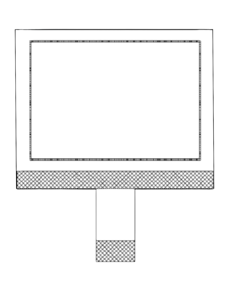
58 x 47 mm LCD Module
- LCD Type: FSTN Positive/Negative
- Viewing Direction: 6:00 O'clock
- Module Size (W x H x T): 58 x 47 x 4.5 mm (Excluded FPC Length)
- Viewing Area (W x H): 53 x 37 mm
- Number of Dots: 128 x 64
- Backlight Type: 3 LEDS White 3.0V 45mA
- Interface Type: Serial Interface
MIC-D5847-01
Digital Power Supply Voltage
Symbol — VDD1
Conditions — - 0.3 - 3.6
Unit — V
Analog Power Supply Voltage
Symbol — VDD2, VDD3
Conditions — - 0.3 - 3.6
Unit — V
LCD Power Supply Voltage
Symbol — V0-XV0
Conditions — -0.3 - 16
Unit — V
LCD Power Supply Voltage
Symbol — VG
Conditions — - 0.3 - 3.6
Unit — V
LCD Power Supply Voltage
Symbol — VM
Conditions — -0.3 - VDD2
Unit — V
Input Voltage
Symbol — Vi
Conditions — -0.3 - VDD1+0.3
Unit — V
Operating Voltage (1)
Symbol — VDD1
Min. / Max. — 1.7 / 3.3
Unit — V
Applicable Pin — VDD1
Operating Voltage (2)
Symbol — VDD2
Min. / Max. — 2.4 / 3.3
Unit— V
Applicable Pin— VDD2
Operating Voltage (3)
Symbol — VDD3
Min. / Max. — 2.4 / 3.3
Unit— V
Applicable Pin— VDD3
Input High-Level Voltage
Symbol — VIHC
Min. / Max. — 0.7 x VDD1 / VDD1
Unit— V
Applicable Pin— MPU Interface
Input Low-Level Voltage
Symbol — VILC
Min. / Max. —VSS1 / 0.3 x VDD1
Unit— V
Applicable Pin— MPU Interface
Output High-Level Voltage
Symbol — VOHC
Condition — IOUT = 1mA, VDD1 = 1.8V
Min. / Max. — 0.8 x VDD1 / VDD1
Unit— V
Applicable Pin— D[7:0]
Output Low-Level Voltage
Symbol — VOLC
Condition — IOUT = 1mA, VDD1 = 1.8V
Min. / Max. — VSS1 / 0.2 x VDD1
Unit— V
Applicable Pin— D[7:0]
Input Leakage Current
Symbol — ILI
Min. / Max. — -1.0 / 1.0
Unit— μA
Applicable Pin— MPU Interface
Output Leakage Current
Symbol — ILO
Min. / Max. — -3.0 / 3.0
Unit— μA
Applicable Pin— MPU Interface
Liquid Crystal Driver ON Resistance
Symbol — RON
Condition 1 — Ta=25°C, VOP = 8.5V / ΔV = 0.85V
- Typical — 0.6
- Max. — 0.8
- Unit— KΩ
- Applicable Pin— COMx
Condition 2 — Ta=25°C, VG = 1.9V, ΔV = 0.19V
- Typical — 1.3
- Max. — 1.5
- Unit— KΩ
- Applicable Pin— SEGx
Frame Frequency
Symbol — FR
Condition — Duty=1/65, VOP=8.5V, Ta = 25°C
Min. / Typical / Max. — 70 / 75 / 80
Unit — Hz
Display Pattern: SNOW (Static)
Symbol — ISS
Condition — VDD1=VDD2=VDD3=3.0V, Booster X5, VOP = 8.5V, Bias=1/9, Ta=25°C
Typical — 150
Max. — 300
Unit — μA
Display OFF
Symbol — ISS
Condition — VDD1=VDD2=VDD3=3.0V, Booster X5, VOP = 8.5V, Bias=1/9, Ta=25°C
Typical — 95
Max. — 190
Unit — μA
Power Down
Symbol — ISS
Condition — VDD1=VDD2=VDD3=3.0V, Ta=25°C
Typical — 8
Max. — 16
Unit — μA
Pin 1
VG — VG is the LCD driving voltage for segment circuits at positive frame
Pin 2
XV0 — XV0 is the LCD driving voltage for common circuits at positive frame
Pin 3
V0 — V0 is the LCD driving voltage for common circuits at negative frame
Pin 4
VSS — Ground
Pin 5
VDD — Power Supply (+3.0)
Pin 6
SDA — Serial Data Input
Pin 7
SCL— Serial Clock Input
Pin 8
A0 — Data or Command Select Signal Input
Pin 9
RES — A Reset Pin
Pin 10
CS — Chip Select Signal Input (Low Active)
Operation Temperature
-20°C to +70°C
Storage Temperature
-30°C to +80°C
MIC-D5847-01
58 x 47 mm LCD Module